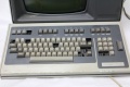
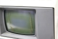
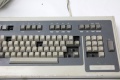
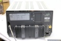
Tektronix 4024
| Tektronix 4024 | |
|---|---|
 | |
| Manufacturer | Tektronix |
| Model | 4024 |
| Lifetime | |
| Introduced | November, 1977 |
| Introductory Price | $2,995 |
| Discontinued | 1982 |
| Communication | |
| Interfaces |
RS-232C, 20 mA current loop |
| Baud Rates | 75, 110, 150, 300, 600, 1200, 2400, 4800, 9600 |
| Display | |
| Size | 12-inch |
| Phosphor | P39 green |
| Refresh Rate | 60 Hz |
| Character Modes | |
| Resolution | 80x34 |
| Matrix | 7x9 |
| Cell | 8x14 |
| Firmware | |
| CPU | Intel 8080 |
| RAM | 4 KB to 32 KB |
The Tektronix 4024 terminal was introduced in 1978 at a price of $2,995.[1][2]
| Part Number | Price | Description |
|---|---|---|
| Option 2 | $230 | Current Loop Interface |
| Option 3 | $300 | RS-232 Peripheral Interface |
| Option 10 | $250 | Polling Interface |
| Option 20 | $250 | 8 KB Display RAM |
| Option 21 | $750 | 16 KB Display RAM |
| Option 22 | $1,750 | 32 KB Display RAM |
| Option 32 | $150 | Ruling Characters |
| Option 48 | No Charge | 220 Volt Power |
| Start | End | Description |
|---|---|---|
0x0000 |
0x00FF |
Power-Up/Interrupt ROM |
0x0100 |
0x07FF |
Unused (1792 bytes) |
0x0800 |
0x0BFF |
I/O Address |
0x0801 |
Processor-Initiated Reset (Not used.) | |
0x0820 |
Host Port Status Word | |
0x0822 |
Host Port USART Data Word | |
0x0823 |
Host Port USART Command/Status Word | |
0x0830 |
Keyboard Port Status Word | |
0x0830 |
Keyboard Port Reset Line | |
0x0830 |
Keyboard Port Data Word | |
0x0C00 |
0x0FFF |
Fix-It ROM |
0x1000 |
0x4FFF |
System Firmware |
0x5000 |
0x7FFF |
Unused (12 KB) |
0x8000 |
0xEFFF |
Additional Display Memory |
0xF000 |
0xFFFF |
Primary Display Memory |
The boards in the system are connected via a motherboard with 2x36 edge card connectors.
| Flip Side | Pin | Pin | Component Side |
|---|---|---|---|
GND |
1- |
-2 |
GND
|
-5V |
3- |
-4 |
-5V
|
SPARE |
5 |
6 |
SPARE
|
-12V |
7- |
-8 |
-12V
|
SPARE |
9 |
10 |
SPARE
|
12V |
11- |
-12 |
12V
|
SPARE |
13 |
14 |
SPARE
|
+5V |
15- |
-16 |
+5V
|
RDIS |
17@ |
18 |
SPARE
|
BA0 |
19# |
#20 |
BA1
|
BA2 |
21# |
#22 |
BA3
|
BA4 |
23# |
#24 |
BA5
|
BA6 |
25# |
#26 |
BA7
|
BA8 |
27# |
#28 |
BA9
|
BA10 |
29# |
#30 |
BA11
|
BA12 |
31# |
#32 |
BA13
|
BA14 |
33# |
#34 |
BA15
|
WACK |
35# |
$36 |
RESET
|
PWDN |
37- |
%38 |
IOADR
|
READ |
39# |
#40 |
WRITE
|
WAIT |
41@ |
@42 |
BRQ
|
BGIN |
43* |
*44 |
BGOUT
|
IA0 |
45% |
%46 |
IA1
|
IA2 |
47% |
@48 |
IRQ
|
LCLK |
49% |
%50 |
HCLK
|
PB0 |
51* |
*52 |
PB1
|
PB2 |
53* |
*54 |
PB3
|
PB4 |
55* |
*56 |
PB5
|
PB6 |
57* |
*58 |
PB7
|
PB8 |
59* |
*60 |
PB9
|
PB10 |
61* |
*62 |
PB11
|
BD0 |
63# |
#64 |
BD1
|
BD2 |
65# |
#66 |
BD3
|
BD4 |
67# |
#68 |
BD5
|
BD6 |
69# |
#70 |
BD7
|
GND |
71- |
-72 |
GND
|
Pin numbers are be annotated with a designation indicating their electrical characteristics as follows:
- |
Power supply pin |
% |
Pin driven by the processor board with no pull up resistor |
$ |
Pin driven by the processor board with a pull up through a 2.7K resistor to +4.3V |
# |
Tri-state pin with a pull up through a 2.7K resistor to +4.3V |
@ |
Open collector pin with a pull up through a 1K resistor to +4.3V |
* |
Non-bused signals which are not necessarily the same at every connector. |
Manx
- 4024 Computer Display Terminal Operator's Manual, January, 1978
- 4024 and 4025 Computer Display Terminals Service Manual (Vol. 1, Theory of Operation), January, 1983
Images


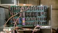
Processor/Comm board
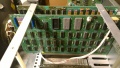
Display Controller board
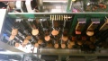
Display Memory board
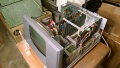
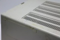
Interior


References
- ↑ "Tektronix 4025 CRT Turns Alphanumerics to Graphics", Computerworld, November 14, 1977, pg. 51
- ↑ "Tektronix Catalog". Tektronix. 1978. http://bitsavers.org/pdf/tektronix/catalog/Tektronix_Catalog_1978.pdf. Retrieved April 17, 2012.
| This article is a stub. You can help the Terminals Wiki by expanding it. |